A Diode is a semiconductor device, two-terminal electronic component that essentially acts as a one-way switch for current. It allows current to flow easily in one direction, but severely restricts current from flowing in the opposite direction.
Diodes are also known as rectifiers because they change alternating current (ac) into pulsating direct current (dc). Diodes are rated according to their type, voltage, and current capacity. Diodes have polarity, determined by an anode (positive lead) and cathode (negative lead). Most diodes allow current to flow only when positive voltage is applied to the anode
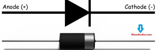
Diode Symbol
The arrowhead points in the direction of conventional current flow in the forward biased condition. That means the anode is connected to the p side and the cathode is connected to the n side.
We can create a simple PN junction diode by doping pentavalent or donor impurity in one portion and trivalent or acceptor impurity in the other portion of silicon or germanium crystal block.
These dopings make a PN junction in the middle part of the block. We can also form a PN junction by joining a p-type semiconductor and n-type semiconductor together with a special fabrication technique. The terminal connected to the p-type is the anode. The terminal connected to the n-type side is the cathode.
Construction of Diode
Diodes can not achieve zero or infinite resistance. Instead, a diode will have negligible resistance in one direction (to allow current flow), and very high resistance in the reverse direction (to prevent current flow). A diode is effectively like a valve for an electrical circuit.

Semiconductor diodes are the most common type of diode. These diodes begin conducting electricity only if a certain threshold voltage is present in the forward direction (i.e. the “low resistance” direction). The diode is said to be “forward biased” when conducting current in this direction. When connected within a circuit in the reverse direction (i.e. the “high resistance” direction), the diode is said to be “reverse biased”.
The diode is said to be “forward biased” when conducting current in this direction. When connected within a circuit in the reverse direction (i.e. the “high resistance” direction), the diode is said to be “reverse biased”.
A diode only blocks current in the reverse direction (i.e. when it is reverse biased) while the reverse voltage is within a specified range. Above this range, the reverse barrier breaks. The voltage at which this breakdown occurs is called the “reverse breakdown voltage”.
When the voltage of the circuit is higher than the reverse breakdown voltage, the diode is able to conduct electricity in the reverse direction (i.e. the “high resistance” direction). This is why in practice we say diodes have a high resistance in the reverse direction – not an infinite resistance.
Working Principle of Diode
A diode’s working principle depends on the interaction of n-type and p-type semiconductors. An n-type semiconductor has plenty of free electrons and a very few numbers of holes. In other words, we can say that the concentration of free electrons is high and that of holes is very low in an n-type semiconductor.
Free electrons in the n-type semiconductor are referred to as majority charge carriers, and holes in the n-type semiconductor are referred to as minority charge carriers.
A p-type semiconductor has a high concentration of holes and a low concentration of free electrons. Holes in the p-type semiconductor are majority charge carriers, and free electrons in the p-type semiconductor are minority charge carriers.
Unbiased Diode
Now let us see what happens when one n-type region and one p-type region come in contact. Here due to concentration differences, majority carriers diffuse from one side to another. As the concentration of holes is high in the p-type region and it is low in the n-type region, the holes start diffusing from the p-type region to the n-type region.

Again the concentration of free electrons is high in the n-type region and it is low in the p-type region and due to this reason, free electrons start diffusing from the n-type region to the p-type region.
The free electrons diffusing into the p-type region from the n-type region would recombine with holes available there and create uncovered negative ions in the p-type region. In the same way, the holes diffusing into the n-type region from the p-type region would recombine with free electrons available there and create uncovered positive ions in the n-type region.
In this way, there would a layer of negative ions in the p-type side and a layer of positive ions in the n-type region appear along the junction line of these two types of semiconductors. The layers of uncovered positive ions and uncovered negative ions form a region in the middle of the diode where no charge carrier exists since all the charge carriers get recombined here in this region. Due to the lack of charge carriers, this region is called the depletion region.
Forward Biased Diode
Now let us see what happens if a positive terminal of a source is connected to the p-type side and the negative terminal of the source is connected to the n-type side of the diode and if we increase the voltage of this source slowly from zero.

In the beginning, there is no current flowing through the diode. This is because although there is an external electrical field applied across the diode, the majority charge carriers still do not get sufficient influence of the external field to cross the depletion region. As we told that the depletion region acts as a potential barrier against the majority charge carriers.
This potential barrier is called forward potential barrier. The majority charge carriers start crossing the forward potential barrier only when the value of externally applied voltage across the junction is more than the potential of the forward barrier. For silicon diodes, the forward barrier potential is 0.7 volt and for germanium diodes, it is 0.3 volt.
When the externally applied forward voltage across the diode becomes more than the forward barrier potential, the free majority charge carriers start crossing the barrier and contribute the forward diode current. In that situation, the diode would behave as a short-circuited path, and the forward current gets limited by only externally connected resistors to the diode.
Reverse Biased Diode
Now let us see what happens if we connect the negative terminal of the voltage source to the p-type side and positive terminal of the voltage source to the n-type side of the diode. At that condition, due to electrostatic attraction of the negative potential of the source, the holes in the p-type region would be shifted more away from the junction leaving more uncovered negative ions at the junction.

In the same way, the free electrons in the n-type region would be shifted more away from the junction towards the positive terminal of the voltage source leaving more uncovered positive ions in the junction.
As a result of this phenomenon, the depletion region becomes wider. This condition of a diode is called the reverse biased condition. At that condition, no majority carriers cross the junction, and they instead move away from the junction. In this way, a diode blocks the flow of current when it is reverse biased.
As we already told at the beginning of this article that there are always some free electrons in the p-type semiconductor and some holes in the n-type semiconductor. These opposite charge carriers in a semiconductor are called minority charge carriers.
In the reverse biased condition, the holes find themselves in the n-type side would easily cross the reverse-biased depletion region as the field across the depletion region does not present rather it helps minority charge carriers to cross the depletion region.
As a result, there is a tiny current flowing through the diode from positive to the negative side. The amplitude of this current is very small as the number of minority charge carriers in the diode is very small. This current is called reverse saturation current.
If the reverse voltage across a diode gets increased beyond a safe value, due to higher electrostatic force and due to higher kinetic energy of minority charge carriers colliding with atoms, a number of covalent bonds get broken to contribute a huge number of free electron-hole pairs in the diode and the process is cumulative.
The huge number of such generated charge carriers would contribute a huge reverse current in the diode. If this current is not limited by an external resistance connected to the diode circuit, the diode may permanently be destroyed.
Types of Diode
The types of diode include:
- Zener diode
- PN junction diode
- Tunnel diode
- Varactor diode
- Schottky diode
- Photodiode
- PIN diode
- Laser diode
- Avalanche diode
- Light emitting diode
Appplication
The application areas of diodes include communication systems as limiters, clippers, gates; computer systems as logic gates, clampers; power supply systems as rectifiers and inverters; television systems as phase detectors, limiters, clampers; radar circuits as gain control circuits, parameter amplifiers, etc.
FAQs:

Hello, Everyone My Name Thilagar And I Am A Website Developer And Blogger We are here to provide update on daily basis about Indian Government Jobs in various sectors, We provide all this information as User-Friendly Content to job Seekers.